- 非IC关键词
深圳市中立信电子科技有限公司

- 卖家积分:
 营业执照:已审核经营模式:贸易/代理/分销所在地区:广东 深圳企业网站:
http://www.zlxele.com
收藏本公司 人气:665093
企业档案
- 相关证件:

- 会员类型:
- 会员年限:13年
- 叶先生

- 电话:0755-23956688
- 手机:13410226883
- 王先生
- 电话:0755-23956688
- 阿库IM:
- 地址:深圳市福田区彩田路彩虹新都大厦彩荟阁7A室
- 传真:0755-23956688
- E-mail:sales@zlxele.com
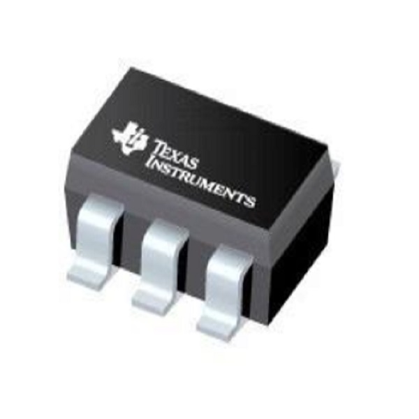


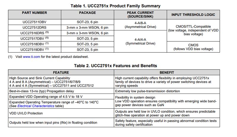
UCC27511DBVR Texas Instruments 门驱动器 4A/8A Sgl Ch Hi-Spd Low-side Gate Driver
SOT-23-6
1 Driver
8 A
9 ns
7 ns
相关产品


产品信息
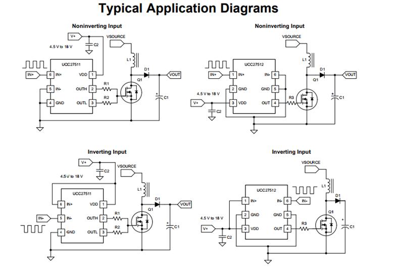
1 Features
• Low-Cost Gate-Driver Device Offering Superior • 6-Pin DBV (SOT-23) and 6-Pin DRS (3-mm ×
Replacement of NPN and PNP Discrete Solutions 3-mm WSON With Exposed Thermal Pad)
• 4-A Peak Source and 8-A Peak Sink Package Options
Asymmetrical Drive
2 Applications • Strong Sink Current Offers Enhanced Immunity
Against Miller Turnon • Switched-Mode Power Supplies
• Split Output Configuration (Allows Easy and • DC-to-DC Converters
Independent Adjustment of Turnon and Turnoff • Companion Gate-Driver Devices for Digital Power
Speeds) in the UCC27511 Saves 1 Diode Controllers
• Fast Propagation Delays (13-ns Typical) • Solar Power, Motor Control, UPS
• Fast Rise and Fall Times (9-ns and 7-ns Typical) • Gate Driver for Emerging Wide Band-Gap Power
• 4.5-V to 18-V Single Supply Range Devices (such as GaN)
• Outputs Held Low During VDD UVLO (Ensures
Glitch-Free Operation at Power Up and Power 3 Description
Down) The UCC27511 and UCC27512 single-channel, highspeed,
low-side gate-driver device can effectively • TTL and CMOS Compatible Input-Logic Threshold drive MOSFET and IGBT power switches. Using a
(Independent of Supply Voltage) design that inherently minimizes shoot-through
• Hysteretic-Logic Thresholds for High-Noise current, UCC27511 and UCC27512 are capable of
Immunity sourcing and sinking high peak-current pulses into
• Dual-Input Design (Choice of an Inverting (IN– capacitive loads offering rail-to-rail drive capability
Pin) and extremely small propagation delay, typically 13 or Noninverting (IN+ Pin) Driver
ns. Configuration)
– Unused Input Pin can be Used for Enable or Device Information(1)
Disable Function PART NUMBER PACKAGE BODY SIZE (NOM)
• Output Held Low When Input Pins Are Floating UCC27511 SOT-23 (6) 2.90 mm x 1.60 mm
• Input Pin Absolute Maximum Voltage Levels Not UCC27512 WSON (6) 3.00 mm x 3.00 mm
Restricted by VDD Pin Bias Supply Voltage
(1) For all available packages, see the orderable addendum at
• Operating Temperature Range of –40°C to 140°C